


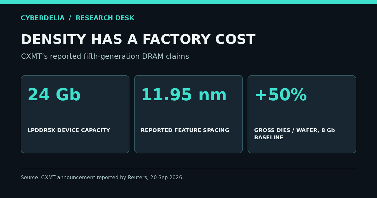
A memory chip does not care whether the world considers its manufacturing route elegant. If the bits fit, the power stays within budget and enough working dies come off the wafer, the product is real. That is the engineering context for CXMT's September 20 announcement: the Chinese memory maker says its fifth-generation DRAM platform is in mass production, with two 24-gigabit LPDDR5X products and denser storage structures made through quadruple patterning.
Reuters reported the company presenting the process at the World Manufacturing Convention in Hefei. CXMT says key features in the memory-cell area are spaced at 11.95 nanometres. It says each new product holds 50 percent more data than its previous equivalent, and that the platform produces at least 50 percent more gross dies per wafer than its fourth-generation process on an 8-gigabit baseline. Those are company claims about particular comparisons. They are not a public, independent benchmark showing that CXMT has matched every performance, yield or cost characteristic of the global leaders.
The interesting story is how a manufacturing constraint becomes a process-development problem. Controls on advanced chipmaking tools can narrow a company's routes to smaller features. They do not repeal the underlying demand for more memory. Engineering answers that pressure with additional patterning steps, process control, simulation, local equipment work and a great deal of effort to make the finished wafer repeatable.
What the new numbers describe
DRAM is working memory. A 24-gigabit device stores 24 billion bits, or about three gigabytes before packaging and marketing conventions complicate the translation. LPDDR5X is the low-power family used prominently in phones and other compact devices. A denser die can fit more capacity into a given package arrangement or allow a manufacturer to cut more candidate dies from a wafer. Both outcomes matter in a market where a small change in cost per good bit can decide whether a part wins a design.
But the three headline numbers are not interchangeable. Feature spacing describes geometry in one part of the device. A 50 percent capacity increase compares the announced 24-gigabit parts with CXMT's earlier equivalent products. A 50 percent increase in gross dies per wafer is a count of potential cut-out chips under the company's stated 8-gigabit baseline. It does not mean 50 percent more working chips were sold from every wafer, because defective dies still have to be discarded. Nor does capacity alone tell us operating speed, power, endurance or system-level competitiveness.
It is easy to make a semiconductor milestone look larger by moving between those denominators without warning. CXMT's announcement may be substantial. Its commercial meaning will become clearer when customers validate the parts, when independent measurements are available and when sustained yield and price are visible. A product described as “in mass production” has crossed an important threshold, but a launch announcement is not a complete factory ledger.
Why quadruple patterning is an engineering detour
Lithography projects a pattern onto a light-sensitive coating. As desired features become finer, a single exposure with available tooling may not provide the necessary detail. Multiple patterning splits a dense design into several simpler passes whose combined features are closer together than one pass would allow. Quadruple patterning increases the number of process steps and the demand for precision. Each additional pass has to align with what came before. Small alignment errors, film variations or etch differences can become a large yield problem when repeated across billions of memory cells.
That is why “they used an older tool four times” is a poor account of the achievement. The difficult part is not just drawing a line four times. It is controlling overlay, defect density, cycle time and cost at factory scale. Extra process steps can consume capacity and make every good die more expensive. A workable route has to recover enough density to outweigh those penalties. Reuters reports CXMT crediting simulations and collaboration with Chinese equipment makers on critical steps. If the company's process yields competitively, those supporting capabilities may be as important as the headline pitch.
Nor does the 11.95-nanometre figure translate directly into a logic-chip “node” or transistor gate length. Memory and logic processes have different structures and naming conventions. The quoted number is spacing of key features in a storage-cell area, as the company describes it. Treating it as proof of parity across all chip fabrication would be marketing arithmetic masquerading as engineering.
The chokepoint moves when someone routes around it
Export restrictions on advanced manufacturing equipment were meant to constrain access to particular production capabilities. CXMT's reported result illustrates a general property of such constraints: they redirect research, capital and manufacturing labor toward alternate paths. A workaround can be slower or more expensive and still be strategically valuable if it creates domestic supply that did not exist before. Its success cannot be measured only by asking whether it beats the best incumbent on every metric today.
For buyers, another credible source of mobile DRAM could alter supplier bargaining and resilience. For competitors, it is a reason to look at actual product qualification and cost. For policymakers, it is evidence that a tooling constraint and a technology freeze are different things. Yet the same announcement leaves large unknowns: yield, wafer cost, customer adoption, sustained output, power under realistic workloads and how much imported equipment or material the route still requires.
There is a useful historical pattern here without pretending history guarantees the outcome. When engineers lose the direct path to a specification, they try to trade process complexity for capability. Sometimes that trade produces a commercially viable chip. Sometimes the extra steps quietly eat the entire gain. The difference appears in factory data, not at a podium.
Why gross dies can flatter a wafer
The company chose a meaningful but incomplete denominator. Gross dies per wafer counts how many chip outlines fit on the wafer before testing. A smaller outline normally allows more candidates. Good dies per wafer is gross dies multiplied by yield, and usable capacity per wafer also depends on whether the product meets its speed, power and reliability targets. A process with 50 percent more gross dies and a substantially lower yield could produce fewer sellable bits. We do not know CXMT's yield from the announcement.
That arithmetic also explains why different capacities need a careful baseline. The stated 50 percent gross-die gain uses an 8-gigabit chip comparison between platform generations; the new product announcement highlights 24-gigabit devices. Comparing the yield or area of those two different density parts directly would muddle the process improvement with the product design. Independent analysts need matching designs and transparent process data to isolate the manufacturing contribution. The company has not published that comparison in the material Reuters described.
A buyer's tests could expose strengths and weaknesses the announcement cannot. Phones care about idle power, thermal behavior, package integration and sustained bandwidth under real workloads. A nominally denser part that passes qualification can reduce board complexity or support larger memory configurations. A part that runs hot or misses supply commitments can lose a design even if the cell geometry is impressive. None of those judgments can be made from feature spacing alone.
What would change the assessment
If independent buyers verify the advertised density and electrical behavior, if volumes remain steady and if defect-adjusted costs compete, this is a meaningful reduction in a manufacturing dependency. If yields are low or the extra exposures make the product too expensive, the nominal density gain could be much less important than the announcement implies. The most revealing future evidence is not a photograph of a wafer; it is qualification data, a production trajectory and price per functioning bit.
CXMT has presented a process claim in a difficult industrial context. The right question is no longer whether engineers can make a 24-gigabit part under constraint. It is whether they can make millions of them predictably, at an acceptable cost, with the speed and power customers need. That is where the geopolitical headline meets the factory floor.
The strongest skeptical reading is straightforward: quadruple patterning is costly, and the announcement reports gross output rather than the number of saleable devices. A challenger can demonstrate sophisticated engineering and still remain behind established suppliers on margins, yield or qualification. The strongest favorable reading is equally concrete: an imperfect domestic route can become a learning platform, generating process knowledge and supplier demand that improve subsequent generations. Both readings require factory evidence. Neither can be settled by comparing promotional node names.
The strategic implication also has a time dimension. A memory part designed into a phone needs a dependable production schedule for the life of that model, not just a working sample at a convention. If a customer commits to a new supplier, packaging, testing and assembly partners must keep pace. That network of qualified processes is harder to build than one successful lithography step and harder for a single export rule to freeze once established. Watching the ecosystem around CXMT may therefore reveal more than watching one chip's nominal feature size.
Quadruple patterning is a route around a manufacturing bottleneck, not a magic cancellation of that bottleneck. CXMT's capacity and gross-die claims deserve attention; yield-adjusted output and customer qualification will decide whether the route changes the memory market.
Source trail and method
CXMT’s September 20, 2026 announcement in Chinese gives the production, patterning, dimensions and package claims. Reuters reported the presentation at the World Manufacturing Convention. Numerical comparisons are attributed to CXMT; the distinction between gross dies and functional yield is Cyberdelia's interpretation of the reported metric.